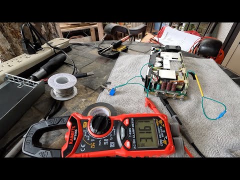
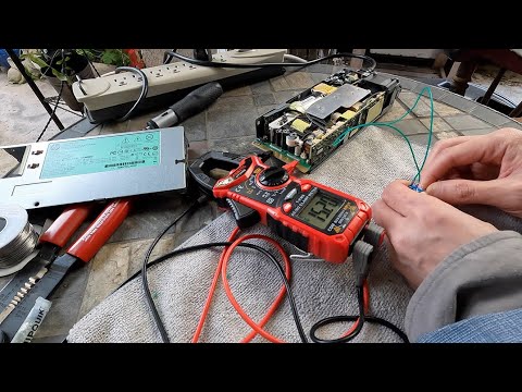
HP HSTNS-PL11/PL30/PL42 1200Watt Hot Plug Power Supply Hack for Vehicle Flashing and Programming. The HPE PSU is a powerful and versatile power supply unit that can be modified or hacked to suit a wide range of needs,With some basic electronics knowledge and proper safety precautions, it's possible to make this PSU even more useful and versatile for your specific applications. Modified HPE PSUs are suitable for RC battery charging, radio power supply, and vehicle flashing/powering applications.
To activate the PSU, add a small resistance resistor between Pin 33 and 36 or simply short them together.
33: ENABLE#
36: PRESENT


LITEON PSU
Pin1 - PGEC
Pin2 - PGED
Pin3 -
Pin4 - GND
Pin5 - Vcc(3.3V)
Delta PSU
Pin1 - GND
Pin2 -
Pin3 - PGED
Pin4 - PGEC
Pin5 - Vcc(3.3V)

- Type III Compensator Using Op-Amp
Type III compensators are a type of compensation network used in control systems to improve stability and performance.
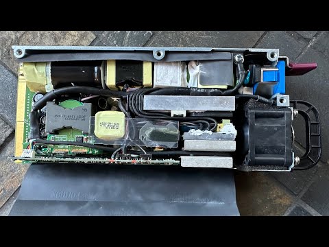
Locate the Type III compensator in the HP PL30 power supply by examining the PCB for the Op-Amp TSV994

To increase the output voltage, one can either increase the reference voltage or decrease the resistance value of R4.


Assuming the default Output is 12.32V.
There are two approaches to prevent the OVP (Over Voltage Protection) from being triggered, one is to add a resistor in parallel with the 01B resistor, the other is to modify the firmware of the MCU(dsPIC33FJ64GS606).
R1 is used to adjust the output voltage of the power supply, while R2 is used to adjust the threshold of the Over Voltage Protection (OVP).
The modification mentioned above is not meant to increase the OVP threshold, but rather to trick the dsPIC33FJ64GS606 MCU into thinking that the output voltage has not been adjusted.
 Figure above shows a current sense amplifier circuit for high side current measurements based on a Texas Instruments OPA2277 op amp and discrete gain setting resistors.
C1,C2,C4 Filter capacitors, GAIN=400.
PL30 Rev10 With Output 14.4V Firmware

PL30 Rev12 AGM Battery Charger 20A Firmware
PL42 Rev01 With Output 14.4V Firmware
 The average current feedback loop is established by cascading a dedicated voltage and current loop compensator, each tied to its respective feedback signal. Just like in peak current mode control, the outer voltage loop compensator output provides the reference for the inner current loop, where a second compensation filter adjusts the average inductor current by adjusting the modulated switch node control signal.
In the PL30, the outer voltage loop is a TYPE III analog compensator. This choice might have been made due to insufficient dsPIC MCU resources to implement a digital solution, or possibly because the analog compensator provides a faster response.
In later power supply designs, with upgraded processors offering more resources, a 3P3Z digital compensator replaced the analog TYPE III compensator, providing improved flexibility and control precision.
At system startup, the secondary-side microcontroller (MCU) transmits the following byte sequence to the primary-side controller:
EA 18 18 18 EA 18 18 18 50 20 00 45 9B 18 18 50 20 00 44 9C 18 18 50 20 00 45 9B 18 18 05 00 00 18 18 18 18 EA 18 18 18 05 02 FE 18 18 18 18 05 04 FC 18 18 18 18 05 06 FA 18 18 18 18 05 08 F8 18 18 18 18 05 1E E2 18 18 18 18 05 22 DE 18 18 18 18 50 28 00 00 D8 18 18 50 2C 00 7E 56 18 18
    mov.w   0x0344, W0        ; Read ADC value (10-bit) into W0
    mov.w   #0x6ac2, W2       ; Load Q15 coefficient (182/(182+39.2+10+4420))/(220/(220+39.2+10+4420)) 0.834 into W2

    ; 16x16 unsigned multiply → 32-bit result in W1:W0 (High:Low)
    mul.uu  W0, W2, W0        ; Perform unsigned multiply, result: W1 = high word, W0 = low word

    ; Shift right by 15 bits to scale back to Q0 (integer)
    ; Equivalent to: (W1 << 1) | (W0 >> 15)
    sl      W1, #0x1, W1      ; W1 = W1 << 1
    lsr.w   W0, #0xf, W0      ; W0 = W0 >> 15
    ior.w   W0, W1, W1        ; Combine bits: W1 = (W1 << 1) | (W0 >> 15)

    ; Final result in W1
    ; W1 = Y = X * 0.834


There are two approaches to prevent the OVP (Over Voltage Protection) from being triggered, one is to connect a resistor in parallel, the other is to modify the firmware of the MCU(PIC16F883).
R3 is used to adjust the output voltage of the power supply, while R4 is used to adjust the threshold of the Over Voltage Protection (OVP).
The modification above is not to increase the OVP threshold, but to make the MCU believe that the output voltage has not been adjusted.
Vdd is the supply voltage of the PIC16F883. By default configuration, The OVP voltage is dependent on the MCU supply voltage, which is approximately 13.86 volts in this case.
PL11 Rev12 Firmware With OVP Disabled

The output voltage of the CT amplified is divided down to 5V and fed into the MCU(PIC16F883). Adding a resistor in parallel across the 8.2k(labeled '8201') resistor can reduce the maximum output current.
A more effective approach would be to measure the voltage at OC_DET along with the actual output voltage of amplifier, and calculate the appropriate divider ratio.
Shorting the 8.2k resistor would cap the maximum output current at around 30A.
The current flowing through the CT(Current Transformer) is transformed into a voltage signal and subsequently amplified using an amplifier. The amplified voltage is directly proportional to the output current
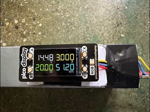
 The image above shows the Raspberry Pi Pico reading data from the HP HSTNS-PL30 power supply via I2C, measuring electrical parameters such as Amps, Volts, Watts, and Watt-hours, and displaying the results on the PIMORONI Pico Display Pack.
| PICO | PL30 |
|---|---|
| VSYS(39) | 5V (12V Standby Input DC DC Converter Output 5V) |
| GND(38) | GND |
| GP4/SDA(6) | 31 |
| GP5/SCL(7) | 32 |
BOMs
- Raspberry Pi Pico
- Pico Display Pack
PICO Firmware 14.48V
The firmware implements a Gain-Scheduled 2P2Z digital compensator with frequency-dependent gain scaling. The controller consists of:
- Second-order feedback (2 poles)
- Second-order error compensation (2 zeros)
- Dynamic gain scheduling based on previous output value
X = d1·u[n-1] + d2·u[n-2]
Y = n1·e[n] + n2·e[n-1] + n3·e[n-2]
Z = (Y · M) >> 7
u[n] = (X + Z) >> 13
d1 = 0x000020F3
d2 = 0xFFFFFF0D
n1 = 0xFFFF0626
n2 = 0x00013663
n3 = 0xFFFFA785
#define Q17_15_SHIFT 15
#define Q17_15_SCALE (1L << Q17_15_SHIFT)
#define Q17_15_FROM_FLOAT(x) ((int32_t)((x) * Q17_15_SCALE))

#define n1 Q17_15_FROM_FLOAT(-1.95197)
#define n2 Q17_15_FROM_FLOAT(2.424896)
#define n3 Q17_15_FROM_FLOAT(-0.69126)
#define d2 Q17_15_FROM_FLOAT(0.25742)
#define d3 Q17_15_FROM_FLOAT(-0.00742)

int32_t mymulsi3(int32_t A, int32_t B)
{
	__asm__ volatile ("mul.su w1,w2,w4");
	__asm__ volatile ("mul.su w3,w0,w6");
	__asm__ volatile ("mul.uu w0,w2,w0");
	__asm__ volatile ("add w4,w1,w1");
	__asm__ volatile ("add w6,w1,w1");

	return(A);
}

	VoltageError = (OUTPUTVOLTAGEREFERENCE -  outputVoltage);

	PIDOutput= mymulsi3((int32_t)n1,VoltageError) + mymulsi3((int32_t)n2,prevVoltageError) + mymulsi3((int32_t)n3,prevVoltageError1);
	PIDOutput = ((PIDOutput >> 7) + mymulsi3((int32_t)d2,PIDOutput1)+mymulsi3((int32_t)d3,PIDOutput2)) >> 13;

	prevVoltageError = VoltageError;		/* Update previous voltage error */
	prevVoltageError1 = prevVoltageError;
	prevVoltageError2 = prevVoltageError1;
	prevVoltageError3 = prevVoltageError2;

	/* Upadation of previous Compensator outputs */
	PIDOutput1= PIDOutput;
	PIDOutput2= PIDOutput1;
	PIDOutput3= PIDOutput2;
The scaling factor M is dynamically calculated:
M = (u[n-1] × 0x44D) >> 15 - 0x4A
M = 0.0336⋅u[n−1]−74
The controller can be written as:


When conducting load testing with ignition ON and AC running, the fan operates at its maximum speed. The output voltage reads 14.28V with no load. However, when under load, there is a voltage drop caused by the impedance in the wires, which is expected. Technically speaking, I would recommend employing Nichrome 80 12 gauge AWG resistance wire for the construction of a dummy load.
PL11/PL30/PL42 Load With Fan on MAX,Audio,High Beam activated

HP HSTNS-PL11 Modification
HP HSTNS-PL30/PL42 Modification
HP HSTNS-PL11 OCP Modification

HP HSTNS-PL30 PICO Watt Meter
HP HSTNS-PL33 Modification

HP HSTNS-PL28 Modification

HP HSTNS-PD19 Modification
HP HSTNS-PD52 Modification